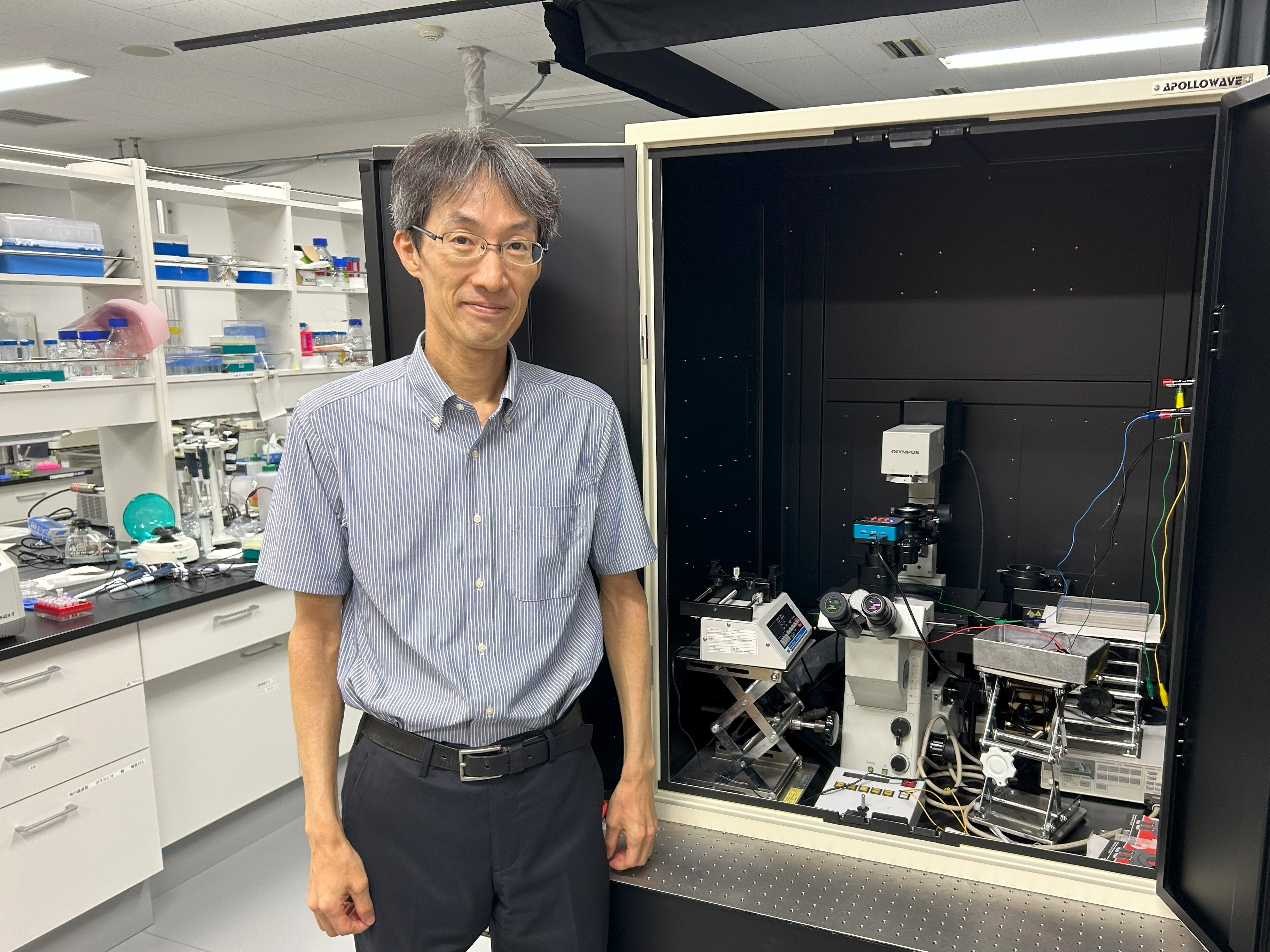
Exploring spatially and temporally resolved deep-ultraviolet spectroscopy toward understanding and controlling optoelectronic properties of ultrawide bandgap semiconductors

Dr. Ryota Ishii

Dr. Ryota Ishii
Assistant Professor
Department of Electronic Science and Engineering, Kyoto University

*The organization and the title are those when awarded

Research summary

Ultrawide bandgap*1 (UWBG) semiconductors have attracted much attention as next-generation semiconducting materials because of their extremely large bandgap. Diamond, gallium oxide (Ga2O3), and aluminum nitride (AlN) are typical examples of UWBG semiconductors, and it is expected that efficient deep-ultraviolet light-emitting devices*2 and ultra-low-loss/high-voltage power devices will be realized using UWBG semiconductors.
However, the luminous efficiency*3 of deep-ultraviolet light-emitting diodes based on UWBG semiconductors is currently very low. Dr. Ishii attributed it to the incomplete understanding of UWBG semiconductor physics, and further focused on the immaturity of deep-ultraviolet spectroscopy*4 which is one of the analysis and measurement techniques for UWBG semiconductors. Dr. Ishii has been investigating the optoelectronic properties of UWBG semiconductors by exploring spatially and temporally resolved deep-ultraviolet spectroscopy. These include the development of a deep-ultraviolet spectroscopic system under perturbation*5 (uniaxial stress/electric) field and a deep-ultraviolet scanning near-field optical microscope*6 operating at the world’s shortest wavelength, the elucidation of the exciton fine structure*7 of AlN, and the observation of a radiative recombination defect in aluminum-gallium-nitride (AlGaN) quantum well structures. These studies should accelerate the development of UWBG semiconductor devices and technologies.

1 Wide Bandgap:
Refers to semiconductors with a large bandgap. The bandgap is a barrier within the semiconductor that electrons cannot pass through, and the wider the bandgap, the more restricted the movement of electrons. It is a crucial factor determining the electrical and optical properties of the semiconductor.
2 Deep-ultraviolet light-emitting device:
A device that emits light in the deep ultraviolet region. The deep ultraviolet region has a very short wavelength and higher energy compared to typical light.
3 Luminous efficiency:
A measure of how much light output a device can achieve relative to the input power supplied to it.
4 Deep ultraviolet spectroscopy:
A technique used to analyze the properties of materials using light in the deep ultraviolet region. By measuring how materials react to deep ultraviolet light, their characteristics and structures can be understood.
5 Perturbation:
The change in external forces or electric fields applied to a system. Under perturbation, the properties and behavior of materials may change.
6 Near-field optical microscope:
A high-resolution microscopy technique that allows the observation of small structures using light at optical wavelengths but using near field techniques to improve the spatial resolution.
7 Exciton fine structure:
The state in which electrons and holes are bound together in a semiconductor material. Excitons are generated by absorbing energy such as light or an electric field, and they possess specific energy states.

Introduction to Research