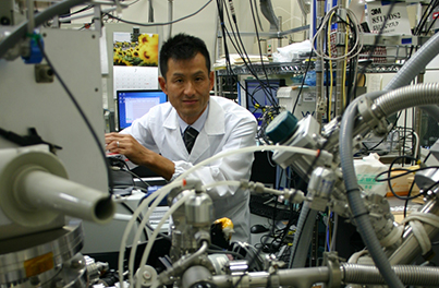
Detection of electronic defects in semiconductor thin-films during plasma processing
Dr. Shota Nunomura, Senior Researcher
Research Center for Photovoltaics, National Institute of Advanced Industrial Science and Technology (AIST)
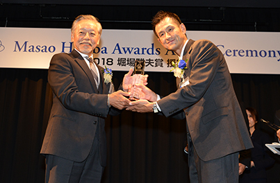
*The organization and the title are those when awarded
DOWNLORD
Research summary
In semiconductor device fabrication, plasma processing technology is widely used for deposition/removal of thin-film materials on/from the wafer. The device performance is strongly influenced by the electronic properties of the films, so that it is necessary to precisely control the plasma processing to achieve high performance of devices. However, the impact of plasma processing on electronic properties of the films has not been elucidated.
Dr. Nunomura has developed a technique for detecting electronic defects during plasma processing, by measuring the photocurrent(*) in the film under illumination of light at two different wavelengths. Using this in-situ real-time technique, he has successively demonstrated the generation and annihilation of electronic defects during the fabrication process.
Although his research work is oriented towards the deposition process of amorphous silicon films for solar cells, it can also be applied to processes using other plasmas.
* Photocurrent is the electronic current in the semiconductor materials, excited by illumination of light. The illumination of light generates free electron-hole pairs in semiconductors.